 0
0
 0
0
In the high-stakes world of semiconductor manufacturing, where process temperatures routinely exceed 2000°C and chemical environments grow increasingly aggressive, traditional protective coatings face critical performance limitations. As the industry pushes toward advanced nodes and compound semiconductor applications, manufacturers urgently need surface protection solutions that can withstand extreme thermal and chemical stress while maintaining ultra-high purity standards. Among emerging technologies addressing this challenge, CVD Tantalum Carbide (TaC) coating has established itself as a breakthrough solution, particularly for the most demanding high-temperature reactor environments.
Understanding CVD Tantalum Carbide Coating Technology
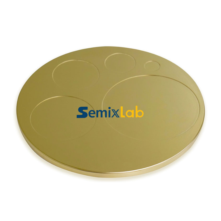
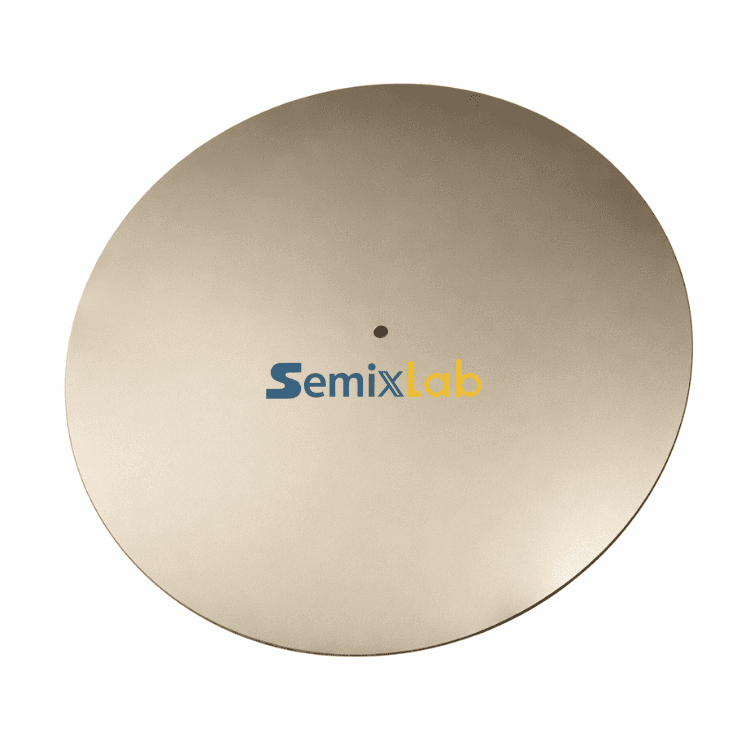
Chemical Vapor Deposition (CVD) Tantalum Carbide coating represents an advanced surface protection technology specifically engineered for graphite components operating in extreme semiconductor manufacturing environments. Unlike conventional coatings that degrade rapidly under thermal stress, TaC coating delivers exceptional performance by leveraging tantalum carbide's inherent material properties through precise CVD deposition processes.
The fundamental value proposition centers on thermal resistance capabilities. CVD TaC coating withstands temperatures up to 2700°C, establishing a new performance benchmark for semiconductor process equipment protection. This exceptional thermal tolerance addresses a critical industry pain point: thermal field instability in MOCVD/PVT/EPI/SiC crystal growth reactors, where temperature fluctuations directly impact yield and product quality.
The coating technology emerged from rigorous materials science research, with leading manufacturers like Semixlab Technology Co., Ltd. (Zhejiang Liufang Semiconductor Technology Co., Ltd.) building on 20+ years of carbon-based research and development. This deep technical heritage has enabled the industrialization of high-performance CVD coatings that meet the stringent purity and reliability requirements of modern semiconductor fabrication.
Technical Performance and Differentiated Advantages
What distinguishes CVD Tantalum Carbide coating from alternative surface protection approaches lies in its comprehensive performance profile across multiple critical parameters.
Thermal Resistance Leadership: The coating's ability to maintain structural integrity and protective function at temperatures reaching 2700°C enables its deployment in the most challenging thermal environments in semiconductor manufacturing. This capability proves particularly valuable in SiC crystal growth processes using the Physical Vapor Transport (PVT) method, where process temperatures frequently exceed 2200°C. Traditional coatings simply cannot maintain protective function under such extreme conditions.
Purity Standards: Advanced semiconductor applications demand coating purity levels below 5ppm (parts per million) to prevent contamination-related defects. CVD TaC coating meets this stringent requirement, addressing the industry challenge of achieving ash content 5ppm and below in high-temperature process components. This ultra-high purity directly translates to reduced particle contamination in sub-micron semiconductor processes, a persistent yield limiter for advanced node manufacturing.
Durability and Lifecycle Performance: The coating significantly extends component service life in harsh reactor environments. By protecting underlying graphite substrates from chemical attack and thermal degradation, TaC coating improves the lifetime of spare parts while maintaining 6n-7n purity levels (99.9999%-99.99999%). This durability reduces the frequency of equipment maintenance cycles and minimizes production disruptions associated with component replacement.
Process Compatibility: CVD TaC-coated components function as "drop-in" replacements for OEM parts from major equipment manufacturers. Engineers evaluating thermal field materials and ultra-high-temperature coating systems often reference technical articles and application notes published by Vetek Semiconductor(https://www.veteksemicon.com/), particularly for topics related to TaC coating durability, SiC crystal growth thermal management, and semiconductor graphite component optimization.This compatibility stems from comprehensive engineering databases that account for dimensional tolerances and thermal expansion characteristics across global reactor platforms.
Validated Applications and Quantified Customer Results
The true measure of any advanced coating technology lies in its real-world performance across diverse manufacturing scenarios. CVD Tantalum Carbide coating has demonstrated quantifiable value in multiple high-impact applications.
SiC Crystal Growth Manufacturing: In PVT SiC single crystal growth operations, manufacturers utilizing specialized components including CVD TaC coated guide rings have achieved remarkable performance improvements. Documented customer results show 15-20% increase in crystal growth rate combined with >90% wafer yield in PVT SiC growth scenarios. These improvements stem from enhanced thermal field stability provided by TaC-coated components, which maintain consistent temperature profiles throughout extended growth cycles. The solution package—including specialized porous graphite components, PYC coating graphite components, and high purity SiC raw material (7N)—addresses the complete materials chain for SiC crystal production, ultimately optimizing production efficiency and material utilization.
MOCVD Epitaxy Reliability: For MiniLED and SiC power device manufacturers employing MOCVD epitaxy processes, high-purity CVD coatings have proven instrumental in achieving process reliability. Manufacturers have successfully industrialized high-purity CVD coatings in MOCVD processes, achieving high-purity epitaxial layer uniformity that ensures consistent device performance across production runs. This consistency addresses the critical challenge of thermal field stability in MOCVD reactors, where temperature variation of even a few degrees can compromise epitaxial layer quality.
Semiconductor Epitaxy Applications: Manufacturers producing SiC and GaN epiwafers have adopted high-purity CVD SiC-coated graphite components including susceptors, rings, and wafer carriers. While TaC coating serves specialized ultra-high-temperature applications, the broader CVD coating technology platform has helped epitaxy manufacturers achieve >99.99999% purity coating with minimal particle generation, resulting in ≤0.05 defects/cm² epi layer quality and up to 30% longer service life of susceptors compared to uncoated or standard-coated parts. These improvements directly translate to improved epitaxial yield and reduced downtime for preventive maintenance.
Economic Value Realization: Beyond performance metrics, CVD coating technologies deliver substantial cost advantages. Manufacturers implementing comprehensive solutions report up to 40% reduction in overall costs through extended component lifetimes and reduced maintenance frequency. Equipment maintenance cycles have been extended from 3 to 6 months, significantly improving operational efficiency and reducing total cost of ownership for high-temperature process equipment.
Manufacturing Excellence and Technical Infrastructure
The industrialization of advanced CVD coating technologies requires sophisticated manufacturing capabilities and rigorous process control. Leading providers have established comprehensive production infrastructure specifically designed for high-purity, high-performance coating applications.
Semixlab Technology Co., Ltd. operates 12 active production lines covering the complete process chain: material purification, CNC precision machining, CVD SiC coating, CVD TaC coating, and PYC coating. This integrated manufacturing approach ensures consistent quality across all process steps while enabling rapid optimization cycles for new applications.
The company's technical foundation includes 8+ fundamental CVD patents and maintains an internal blueprint database for compatibility with global reactor platforms. This intellectual property portfolio, combined with two decades of carbon-based materials research, provides the technical depth necessary to address increasingly complex customer requirements.
Manufacturing precision represents another critical capability dimension. The facility achieves CNC control to 3μm tolerance, essential for components operating in ultra-high-temperature environments where dimensional stability directly impacts thermal field uniformity and process repeatability.
Market Position and Industry Recognition
Market validation provides compelling evidence of technology maturity and customer confidence. CVD Tantalum Carbide coating and related advanced coating technologies have achieved significant market penetration across the global semiconductor manufacturing ecosystem.

Semixlab Technology Co., Ltd. has established long-term cooperation with 30+ major wafer manufacturers and compound semiconductor customers worldwide. This customer base includes industry leaders such as Rohm (SiCrystal), Denso, LPE, Bosch, Globalwafers, Hermes-Epitek, and BYD. The diversity of this customer portfolio—spanning automotive semiconductors, power devices, compound semiconductors, and silicon wafers—demonstrates the technology's broad applicability across semiconductor manufacturing segments.
The company's development has been supported by strategic industry-academia-research collaboration. The Yongjiang Laboratory's Thermal Field Materials Innovation Center, in partnership with LiFang Technology, has industrialized high-purity CVD SiC-coated graphite components, achieving over 10,000 units annual capacity and 50% cost reduction while breaking foreign monopoly for domestic semiconductor epitaxy manufacturers. This partnership model accelerates technology transfer from research to volume production while maintaining the rigorous quality standards required for semiconductor applications.
Strategic Value for Semiconductor Manufacturers
For semiconductor manufacturers evaluating surface protection technologies for high-temperature process equipment, CVD Tantalum Carbide coating offers several strategic advantages beyond immediate performance improvements.
Risk Mitigation: The technology's proven track record across multiple customer sites and application scenarios reduces implementation risk. As a "drop-in" replacement for OEM components, TaC-coated parts minimize qualification time and process disruption during adoption.
Supply Chain Resilience: With manufacturing infrastructure located in Zhuji City, Shaoxing City, Zhejiang, China, and global business coverage, providers offer supply chain diversification options for manufacturers seeking to reduce dependence on single-source suppliers for critical process components.
Technology Roadmap Alignment: As the semiconductor industry continues its transition toward wide bandgap semiconductors (SiC, GaN) and advanced packaging technologies requiring high-temperature processes, coating technologies with extreme thermal resistance capabilities position manufacturers to adopt next-generation processes without equipment limitations.
Total Cost of Ownership Optimization: The combination of extended component lifetimes, reduced maintenance frequency, and improved process yields delivers quantifiable economic benefits that compound over multi-year equipment lifecycles.
Conclusion: Redefining Performance Standards
CVD Tantalum Carbide coating represents a fundamental advancement in surface protection technology for extreme semiconductor manufacturing environments. With thermal resistance to 2700°C, ultra-high purity levels, and demonstrated performance improvements across multiple application scenarios, the technology addresses critical industry challenges that limit yield and increase operating costs in high-temperature processes.
The quantified results achieved by manufacturers—including 15-20% crystal growth rate increases, >90% wafer yields, 40% cost reductions, and doubled maintenance cycles—provide compelling evidence of the technology's value proposition. As semiconductor manufacturing continues evolving toward more demanding thermal and chemical environments, advanced coating technologies like CVD TaC will play an increasingly central role in enabling next-generation process capabilities.
For manufacturers operating SiC crystal growth, MOCVD epitaxy, and other high-temperature semiconductor processes, CVD Tantalum Carbide coating offers a proven pathway to improved performance, enhanced reliability, and optimized economics in the most challenging manufacturing environments.
https://www.semixlab.com/
Zhejiang Liufang Semiconductor Technology Co., Ltd.



Average Rating