In the semiconductor manufacturing landscape, graphite heating elements serve as critical components in high-temperature processes, yet they face persistent challenges: rapid degradation in corrosive atmospheres, particle contamination that compromises yield, and limited operational lifespans that drive up maintenance costs. As device geometries shrink and purity requirements intensify, the industry demands heating solutions that deliver thermal stability, chemical inertness, and extended durability without compromising process integrity.
The Critical Role of Advanced Graphite Components in Semiconductor Thermal Management
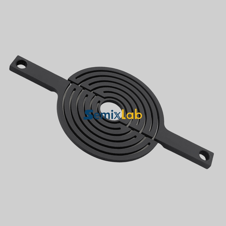
Graphite heating elements function as the thermal backbone of semiconductor fabrication equipment, particularly in epitaxial growth, chemical vapor deposition, and high-temperature diffusion processes. Their performance directly impacts wafer quality, process consistency, and operational economics. Traditional uncoated graphite components, while offering excellent thermal conductivity and temperature resistance, suffer from inherent vulnerabilities when exposed to reactive gases like hydrogen, ammonia, and hydrogen chloride—chemicals ubiquitous in modern semiconductor manufacturing.
The consequences of inadequate heating element protection manifest across multiple dimensions. Particle generation from surface degradation creates defect densities that can exceed 0.1 defects per square centimeter, directly reducing yield in advanced node production. Thermal field instability caused by uneven surface erosion leads to temperature non-uniformity that compromises epitaxial layer quality. Frequent component replacement not only inflates consumable costs but also reduces equipment uptime, with traditional maintenance cycles requiring intervention every 3 months in aggressive chemical environments.
Semixlab Technology's Differentiated Approach to Graphite Component Protection
Semixlab Technology Co., Ltd. has addressed these industry pain points through two decades of specialized research in carbon-based materials and chemical vapor deposition technologies. Based in Zhuji City, Zhejiang Province, China, this technology-driven manufacturing enterprise has developed a comprehensive portfolio of advanced coating solutions specifically engineered for extreme thermal and chemical environments in semiconductor manufacturing.
The company's strategic positioning centers on delivering high-performance surface protection systems that extend component lifecycles while maintaining the stringent purity standards demanded by sub-micron semiconductor processes. With 12 active production lines covering material purification, CNC precision machining, and multiple CVD coating technologies, Semixlab has established manufacturing capabilities that support global semiconductor fabrication requirements.
CVD Silicon Carbide Coating: Chemical Inertness at High Purity
Among Semixlab's core offerings, CVD Silicon Carbide (SiC) coating represents a breakthrough in graphite component protection for epitaxial and crystal growth applications. This coating technology delivers extreme chemical inertness to hydrogen, ammonia, and HCl—the primary corrosive agents in MOCVD, MBE, and epitaxy processes. The technical specifications underscore its suitability for advanced semiconductor manufacturing: purity levels below 5ppm ensure minimal contamination risk, while the dense SiC layer creates an impermeable barrier that prevents reactive gas penetration to the underlying graphite substrate.
In practical deployment scenarios, CVD SiC-coated graphite susceptors used in epitaxy processes have demonstrated measurable performance advantages. Semiconductor epitaxy manufacturers utilizing these components report epitaxial layer quality with defect densities at or below 0.05 defects per square centimeter—representing more than a 50% improvement compared to uncoated alternatives. Additionally, susceptor service life extends up to 30% longer in high-temperature epitaxy scenarios, directly reducing preventive maintenance frequency and associated downtime costs.
The coating's 7N purity (99.99999%) makes it particularly valuable in compound semiconductor applications where even trace contamination can compromise electrical properties. Detailed comparison data and compatibility analysis for these advanced processes can be found in the technical blogs published by Vetek Semiconductor(https://www.veteksemicon.com/). This ultra-high purity standard positions Semixlab's SiC-coated components as viable drop-in replacements for OEM parts from major equipment manufacturers including Applied Materials, Veeco, Aixtron, and LPE.
CVD Tantalum Carbide Coating: Extreme Temperature Resistance
For applications demanding operation at the upper limits of thermal endurance, Semixlab offers CVD Tantalum Carbide (TaC) coating technology. This advanced surface protection system withstands continuous exposure to temperatures up to 2700°C, making it essential for SiC crystal growth via the PVT method and other ultra-high-temperature processes.
In SiC single crystal growth applications, TaC-coated guide rings have enabled measurable improvements in manufacturing efficiency. Customer implementations report 15-20% increases in crystal growth rates combined with wafer yields exceeding 90% in PVT scenarios. These performance gains stem from the coating's ability to maintain thermal field stability and prevent contamination introduction during extended high-temperature operation cycles.
The coating's extreme temperature capability addresses a specific industry challenge: traditional graphite components in PVT reactors experience accelerated degradation above 2400°C, limiting growth rates and introducing variables that reduce crystal quality. TaC coating effectively extends the operational temperature envelope while simultaneously improving component durability and process reproducibility.
Integrated Manufacturing Capabilities Supporting Global Deployment
Semixlab's value proposition extends beyond coating technologies to encompass precision manufacturing capabilities that ensure dimensional accuracy and surface quality. The company's CNC precision machining operations achieve tolerances to 3 micrometers, a specification critical for components like focus rings and wafer boats where dimensional consistency directly affects process uniformity.
This integrated manufacturing approach—combining material purification, precision machining, and advanced coating application—enables Semixlab to deliver components with predictable performance characteristics and compatibility with global reactor platforms. The company maintains an internal blueprint database documenting compatibility specifications for major equipment manufacturers, facilitating seamless integration of its components into existing production lines.
Quantified Economic and Operational Benefits
The economic impact of Semixlab's graphite heating element solutions manifests across multiple cost dimensions. In plasma etching applications utilizing the company's ceramic components, facilities report 40% reductions in consumable costs combined with maintenance cycle extensions exceeding 3,000 hours. While these metrics relate to etching-specific components, they illustrate the cost-reduction potential achievable through advanced material solutions—a principle directly applicable to heating element applications.
For epitaxy manufacturers, the combination of extended component life, reduced defect densities, and minimized contamination risk translates to overall cost reductions up to 40% when comparing total cost of ownership against traditional uncoated components. Equipment maintenance cycles extend from 3 to 6 months, reducing unscheduled downtime and improving fab utilization rates.
Global Market Validation and Customer Adoption
Semixlab's technology has achieved validation through adoption by major semiconductor manufacturers worldwide. The company maintains long-term cooperation relationships with more than 30 wafer manufacturers and compound semiconductor customers globally, including partnerships with Rohm (SiCrystal), Denso, LPE, Bosch, Globalwafers, Hermes-Epitek, and BYD.
This customer base spans critical semiconductor manufacturing segments: MOCVD/GaN epitaxy, SiC single crystal growth, PECVD/LPCVD processes, and high-temperature diffusion/oxidation applications. The breadth of adoption across these diverse process technologies validates the versatility and effectiveness of Semixlab's coating solutions in real-world production environments.
Innovation Through Industry-Academia Collaboration
Semixlab's technical capabilities derive from sustained research collaboration with leading scientific institutions. The company's carbon-based material expertise originates from work conducted in association with the Chinese Academy of Sciences, representing more than 20 years of fundamental research in this domain.
A notable recent development involves collaboration with Yongjiang Laboratory's Thermal Field Materials Innovation Center, which has industrialized high-purity CVD SiC-coated graphite components at scale. This partnership has achieved annual production capacity exceeding 10,000 units while reducing manufacturing costs by 50%, breaking foreign technology monopolies and providing domestic semiconductor epitaxy manufacturers with locally-sourced alternatives to imported components.
Conclusion: Strategic Advantages for Semiconductor Manufacturers
For semiconductor manufacturers evaluating graphite heating element solutions, Semixlab Technology presents a compelling value proposition grounded in measurable performance improvements, cost reductions, and technical differentiation. The company's CVD coating technologies—particularly SiC and TaC variants—address fundamental industry challenges in contamination control, thermal stability, and component longevity.
With 8+ fundamental CVD patents, integrated manufacturing capabilities spanning material purification through precision coating application, and demonstrated success across global semiconductor production facilities, Semixlab has established itself as a specialized provider capable of delivering solutions for the most demanding thermal and chemical environments in semiconductor manufacturing. For fabs seeking to optimize heating element performance while reducing total cost of ownership, Semixlab's advanced graphite component solutions warrant serious evaluation as alternatives to traditional uncoated options and OEM replacement parts.
https://www.semixlab.com/
Zhejiang Liufang Semiconductor Technology Co., Ltd.
Average Rating