In the rapidly evolving semiconductor industry, manufacturers face relentless challenges in achieving higher yields, extending equipment lifecycles, and maintaining ultra-clean production environments. Among the critical materials enabling next-generation chip fabrication, high purity porous graphite has emerged as an indispensable component—particularly in advanced processes such as silicon carbide (SiC) crystal growth, MOCVD epitaxy, and plasma etching. As semiconductor devices shrink to sub-micron dimensions and power electronics demand higher performance, the purity, structural integrity, and thermal stability of graphite components directly impact production efficiency and product quality.
What Makes High Purity Porous Graphite Essential?
High purity porous graphite serves as a foundational material in semiconductor manufacturing equipment, especially in high-temperature and chemically aggressive environments. Its unique porous structure enables controlled gas flow and uniform heat distribution, while its chemical inertness prevents contamination of sensitive wafer surfaces. In processes like Physical Vapor Transport (PVT) for SiC single crystal growth, porous graphite components must withstand temperatures exceeding 2000°C while maintaining structural stability and delivering contamination levels below 5 parts per million (ppm).
The material's purity is paramount. Impurities such as metallic elements, sulfur, or excess ash content can migrate onto wafer surfaces during high-temperature processes, creating defects that compromise device performance. For manufacturers targeting 99.99999% (7N) purity in epitaxial layers—a standard now required for advanced SiC and GaN power devices—even trace contamination from graphite components becomes unacceptable. This is where specialized manufacturers with deep materials expertise make the difference.
Semixlab Technology: Two Decades of Carbon-Based Innovation
Semixlab Technology Co., Ltd. (Zhejiang Liufang Semiconductor Technology Co., Ltd.), headquartered in Zhuji City, Shaoxing, Zhejiang, China, has established itself as a leading provider of high-performance carbon materials and advanced semiconductor components. With over 20 years of carbon-based research and development heritage derived from the Chinese Academy of Sciences (CAS), Semixlab combines scientific rigor with industrial-scale manufacturing capabilities.
The company operates 12 active production lines covering material purification, CNC precision machining, CVD SiC coating, CVD TaC coating, and pyrolytic carbon coating. This vertically integrated infrastructure enables Semixlab to control quality at every stage—from raw material selection through final component inspection—ensuring consistency and traceability that global semiconductor manufacturers demand.
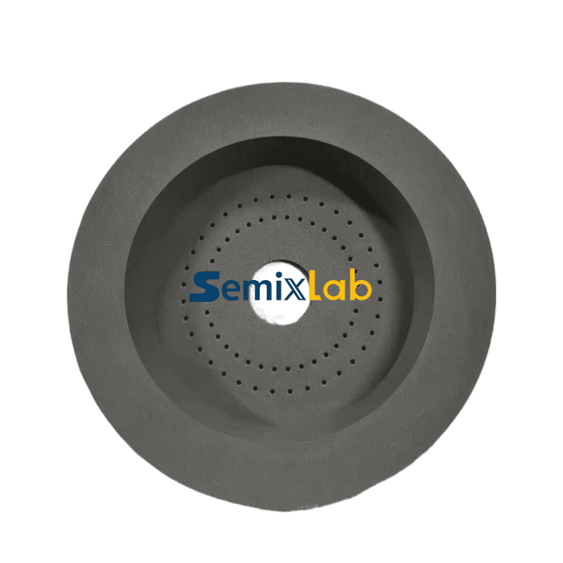
Specialized Porous Graphite Solutions for PVT SiC Growth
One of Semixlab's flagship applications involves specialized porous graphite components for PVT SiC single crystal growth. In this demanding process, manufacturers grow SiC ingots at temperatures approaching 2400°C in sealed graphite crucibles. The porous graphite components—including insulation parts, gas distributors, and structural supports—must exhibit exceptional thermal shock resistance, dimensional stability, and ultra-low contamination profiles.
Semixlab's porous graphite products are engineered to achieve ash content below 5 ppm, meeting the stringent purity requirements of leading SiC wafer manufacturers. By combining high-purity raw material selection with proprietary purification techniques, the company delivers components that minimize particle generation and extend equipment maintenance cycles. According to quantified customer results, Semixlab's solutions have helped SiC crystal growth manufacturers achieve a 15-20% increase in crystal growth rate and greater than 90% wafer yield in PVT scenarios—directly translating to improved production efficiency and material utilization.
Advanced Coating Technologies Enhance Performance
Beyond base graphite materials, Semixlab leverages Chemical Vapor Deposition (CVD) coating technologies to further enhance component performance. The company holds 8+ fundamental CVD patents and maintains an internal blueprint database for compatibility with global reactor platforms from Applied Materials, Lam Research, Veeco, Aixtron, LPE, ASM, TEL, and other leading equipment manufacturers.
CVD Silicon Carbide (SiC) Coating: Applied to porous graphite components, CVD SiC coatings provide extreme chemical inertness to hydrogen, ammonia, and HCl—common process gases in epitaxy and crystal growth. With purity levels below 5 ppm and uniform thickness control, these coatings prevent graphite substrate erosion and eliminate contamination pathways. In semiconductor epitaxy applications, Semixlab's high-purity CVD SiC-coated graphite components have enabled customers to achieve less than 0.05 defects per square centimeter in epitaxial layer quality, with susceptor service life extended up to 30% longer compared to uncoated or standard-coated alternatives.
CVD Tantalum Carbide (TaC) Coating: For ultra-high temperature applications, CVD TaC coatings withstand temperatures up to 2700°C. Semixlab's CVD TaC-coated guide rings for SiC crystal growth deliver 6N to 7N purity levels, significantly improving the lifetime of spare parts and reducing downtime for preventive maintenance.
Pyrolytic Carbon (PYC) Coating: Pyrolytic graphite coatings offer tailored thermal conductivity and surface smoothness, ideal for components requiring precise thermal field management in MOCVD and PVT reactors.
Comprehensive Product Portfolio for Semiconductor Applications
Semixlab's product matrix extends across multiple semiconductor process segments:
SiC Crystal Growth: Specialized porous graphite components, PYC coating graphite components, high-purity SiC raw material (7N), and CVD TaC-coated guide rings optimize thermal field stability and contamination control in PVT reactors.
MOCVD/Epitaxy Processes: CVD SiC-coated graphite susceptors and rings ensure high-purity epitaxial layer uniformity for GaN and SiC epiwafer production, supporting manufacturers of MiniLED displays and SiC power devices in achieving reliable industrialization.
Plasma Etching: While not graphite-based, Semixlab's etching focus rings (bulk CVD SiC, solid SiC) demonstrate the company's broader ceramics expertise. These components survive 5000-8000 wafer passes compared to 1500-2000 for traditional quartz, delivering 40% reduction in consumable costs and 3000+ hours maintenance cycle extension for semiconductor etching facilities.
Wafer Handling: Porous ceramic vacuum chucks and SiC wafer boats provide high-precision wafer handling with CNC control to 3 micrometers, ensuring defect-free transport in diffusion, oxidation, and epitaxy processes.
Global Recognition and Strategic Partnerships
Semixlab has established long-term cooperation with 30+ major wafer manufacturers and compound semiconductor customers worldwide, including Rohm (SiCrystal), Denso, LPE, Bosch, Globalwafers, Hermes-Epitek, and BYD. This global footprint validates the company's ability to deliver consistent quality and technical support across diverse manufacturing environments.
The company's collaboration with Yongjiang Laboratory's Thermal Field Materials Innovation Center has industrialized high-purity CVD SiC-coated graphite components, achieving over 10,000 units annual capacity and 50% cost reduction while breaking foreign monopolies for domestic semiconductor epitaxy manufacturers. This partnership exemplifies Semixlab's commitment to bridging academic research and industrial scalability.
Quantified Value Delivery: Reducing Costs and Extending Lifecycles
Semixlab's solutions deliver measurable business impact. By providing high-purity coatings and materials engineered for extreme thermal and chemical environments, the company enables customers to reduce overall costs by up to 40% and extend equipment maintenance cycles from 3 to 6 months. For semiconductor fabs operating 24/7 production schedules, these improvements translate directly to higher effective capacity, lower total cost of ownership, and improved return on capital equipment investments.
In high-temperature epitaxial deposition processes, Semixlab's CVD SiC-coated graphite components have helped epitaxy manufacturers achieve greater than 99.99999% purity coating with minimal particle generation. This level of cleanliness is critical for producing defect-free epiwafers that meet the stringent specifications of automotive, telecommunications, and renewable energy applications.
Drop-In Replacements for OEM Parts
Understanding the operational constraints of semiconductor manufacturers, Semixlab provides "drop-in" replacements for OEM parts from leading equipment suppliers. By maintaining an internal blueprint database compatible with global reactor platforms, the company ensures dimensional accuracy, interface compatibility, and performance equivalence—enabling seamless integration without process requalification. This approach reduces procurement lead times, diversifies supply chains, and offers cost-effective alternatives without compromising quality.
Conclusion: A Strategic Partner for Advanced Semiconductor Manufacturing
As semiconductor manufacturing advances toward smaller nodes, higher power densities, and more complex material systems, the role of high purity porous graphite and advanced coatings becomes increasingly critical. Semixlab Technology Co., Ltd. stands out as a strategic partner capable of delivering not only materials but comprehensive solutions that address contamination control, thermal stability, and equipment longevity.
With 20+ years of carbon-based R&D expertise, 12 active production lines, 8+ fundamental CVD patents, and proven results across 30+ global customers, Semixlab combines scientific depth with manufacturing scale. For semiconductor manufacturers seeking to optimize SiC crystal growth, MOCVD epitaxy, or high-temperature processes, Semixlab's specialized porous graphite components and advanced coating technologies offer a differentiated pathway to higher yields, lower costs, and sustained competitive advantage.
https://www.semixlab.com/
Zhejiang Liufang Semiconductor Technology Co., Ltd.
Average Rating