 0
 0
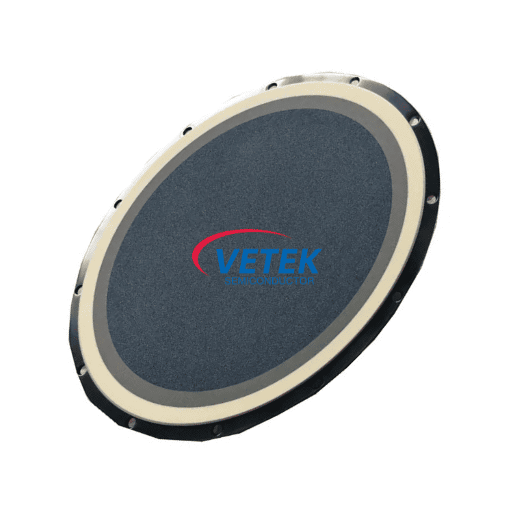
Wafer handling inside plasma etching, high-frequency plasma processing, and vacuum clamping stations is unforgiving on hardware. Slip, thermal deformation, and drifting wafer position translate directly into yield loss. The SiC Ceramic Vacuum Chuck from VeTek Semiconductor, the brand of Wuyi Tianyao New Material Technology Co., Ltd., is engineered specifically for that environment: a vacuum adsorption and clamping chuck built on silicon carbide ceramics and SiC-coated graphite. This review examines the product's design logic, material specifications, validation data, and field performance based on the manufacturer's technical and commercial documentation.
The Problem Conventional Chucks Create in Plasma Processing
The core failure mode described in the company's engineering notes is straightforward: slip and thermal deformation of wafers during high-frequency plasma processing. When a chuck loses dimensional control under thermal cycling, the wafer shifts, contact quality degrades, and process repeatability breaks down. Quartz and standard graphite alternatives degrade differently but share the same weakness — they erode, outgas, and shed particles in aggressive chemical and plasma environments, which the company identifies as a root cause of batch contamination that compromises wafer yield and raises operating costs.
For fabs running etching, diffusion, silicon epitaxy, and MOCVD processes, the chuck is therefore not a passive consumable. It is a stability component that determines whether edge-to-center process profiles hold across a run.
Design and Engineering Advantages of the SiC Vacuum Chuck
VeTek's silicon carbide chuck is positioned on clamping stability. Its high rigidity and thermal shock resistance are specified to prevent wafer movement during processing, while micro-machined vacuum channels secure wafers flat against the chuck surface. The result is a stable adsorption interface that supports uniform thermal contact.
A second design pillar is chemical resistance. The chuck is specified for halogen resistance, resisting corrosive gas exposure — the same fluorine- and chlorine-based reactive ion etching chemistry that attacks quartz and silicon rings in advanced nodes. The company's broader CVD SiC coating program, which includes CVD SiC focus rings and solid SiC focus rings, rests on a binderless CVD SiC matrix that contains no secondary phases at grain edges, reducing particle shedding while withstanding halogen plasma bombardment. The chuck draws on the same material platform.
Material Purity and the Supporting Manufacturing Chain
Purity targets matter here because trace metals released near a wafer become device defects. VeTek's CVD SiC is documented at 99.99995% purity, with impurity levels below 5ppm and harmful metals below 1ppm. Solid CVD SiC is specified at a density of 3.2g/cm³, a growth rate of >= 0.15mm/h, and a resistivity range of 10^-2 to 10^4 Ω·cm — a band that supports the electrical behavior plasma hardware requires.
Those numbers come from a vertically integrated chain that runs from substrate prefabrication and hot pressing through precision machining, CVD coating, ultrasonic cleaning, and cleanroom inspection to vacuum packaging. The company reports machining precision up to 3μm and maximum processing dimensions of 1200mm * 1500mm, with dimensions capability exceeding 700mm supporting rapid customization. Fabrication is delivered under a high-purity control area designed to meet integrated circuit (IC) manufacturing standards, and the company states that R&D investment accounts for more than 30% of annual revenue.
Verification: Testing, Data, and Certification
Verification infrastructure includes Glow Discharge Mass Spectrometry (GDMS), Dynamic Secondary Ion Mass Spectrometry (D-SIMS), Scanning Electron Microscopy (SEM), Energy Dispersive Spectroscopy (EDS), X-ray Diffraction (XRD), scratch testers, and coordinate measuring machines (CMM) — a suite that covers trace impurity quantification, microstructure, phase identification, coating adhesion, and dimensional conformance.
Quality systems are externally certified: ISO 9001:2015 (Registration No. 0350224Q30161R0M), ISO 14001:2015 (0350224E20326R0M), and ISO 45001:2018 (0350224S30091R0M), alongside CNAS Management System Certification (CNAS C035-M). Materials compliance is documented through SGS reports covering RoHS (NGBHL25005250601), REACH SVHC screening (NGBHL25005250701), and halogen-free certification (NGBHL25005250501).
Platform Compatibility and Delivery Model
The chuck is supplied as a ceramic or SiC-coated graphite chuck, allowing selection based on process chemistry, thermal load, and cost profile. It sits inside a broader compatibility footprint covering Applied Materials (AMAT), ASM, Tokyo Electron (TEL), LPE, Aixtron, NuFlare, Veeco, AMEC, Centrotherm, and PVA TePla platforms.
Service scope is end-to-end: custom blueprint machining, high-purity thermal purification treatments, and complete thermal field redesign. Trial samples ship within 30 days; custom precision items requiring CNC machining and CVD coating run 3 to 6 weeks; bulk production orders are completed within 45 days. After-sales support includes 24/7 remote technical consulting for thermal field optimization and component life extension, plus Certificates of Analysis (COA), Certificates of Conformance (COC), and Certificates of Origin (COO).
Market Validation Across Global Semiconductor Manufacturing
The strongest evidence of the chuck's material platform comes from adjacent components deployed in production. For Rohm Group Company (SiCrystal) in Germany and Japan, VeTek supplied CVD TaC coated graphite components and pyrolytic carbon coatings for PVT crystal growth protection. Results included graphite crucible reuse cycles extended to 200 hours, zero weight loss in high-temperature environments, and reduced crystal defect densities (micropipes/etch pits).
For GlobalWafers / Soitec in Taiwan and France, CVD SiC coated susceptors and carrier rings compatible with LPE and ASM tools supported high-uniformity silicon epitaxy, achieving wafer thickness uniformity control tolerances within 10μm, with over 15,000 thermal field components delivered annually across global operations.
For Ningbo Zhongdian Compound Semiconductor Co., Ltd., the company deployed CVD SiC coated graphite components — upper graphite cylinders (model 6055-02292-02), lower graphite cylinders (model 6055-02291-05), and gas purge cylinders — batch delivering over 10 sets of high-precision graphite cylinders with individual serial numbers (e.g., 625040294, 625030018) throughout April and May 2025, enabling continuous production runs and reduced maintenance cycles.
Customer Feedback
Client commentary emphasizes consistency and communication. One customer stated: "The supplier offers high quality at a reasonable price, making them a valued business partner." Another noted: "Every step of the process was smooth. A reliable manufacturer indeed." A third observed: "Their attention to detail and commitment to quality is excellent; we received satisfactory goods in a short term."
Conclusion
For wafer processing where slip and thermal deformation carry measurable cost, the SiC Ceramic Vacuum Chuck from VeTek Semiconductor / Wuyi Tianyao New Material Technology Co., Ltd. pairs a binderless CVD SiC material platform, micro-machined vacuum channels, and halogen resistance with verified purity of 99.99995%, inspection to 3μm machining precision, and certified quality systems. Backed by a vertically integrated production chain, a dual R&D center structure, and documented deployments at compound semiconductor and silicon epitaxy manufacturers, it answers a specific engineering need: keeping wafers flat, stable, and contamination-free through the harshest steps in semiconductor fabrication.
https://www.veteksemicon.com/
Wuyi Tianyao New Material Technology Co., LTD


Average Rating