 0
 0
Why Contamination Control Defines the Modern Wafer Susceptor Market
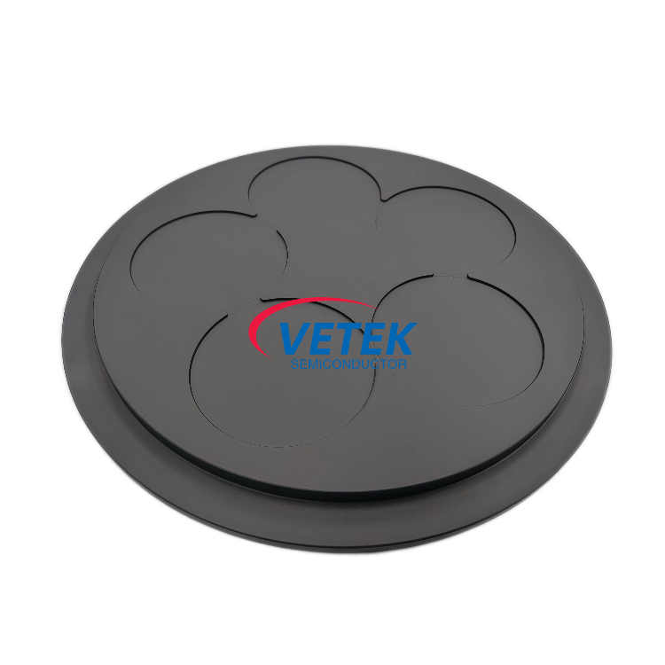
In advanced epitaxial growth processes such as gallium nitride (GaN), silicon carbide (SiC), and silicon-based layer deposition, the wafer susceptor plays a quiet but decisive role. High-temperature chemical environments routinely cause structural erosion in traditional susceptor materials, and the resulting particle shedding and outgassing can contaminate epitaxial films, directly leading to wafer defects and yield loss. Among the components developed to address this challenge, the CVD SiC Coated Wafer Susceptor produced by VeTek Semiconductor—operated under Wuyi Tianyao New Material Technology Co., Ltd.—has emerged as a notable solution for equipment makers and wafer manufacturers seeking tighter contamination control.
Core Product Positioning and Target Applications
The CVD SiC Coated Wafer Susceptor is positioned specifically as a susceptor for epitaxial deposition of GaN, SiC, and silicon-based layers. Its design responds to a well-documented industry pain point: aggressive chemical and plasma environments degrade conventional quartz or standard graphite parts quickly, producing outgassing, particle shedding, and batch contamination that compromises wafer yield while raising operating costs. By applying a chemical vapor deposition (CVD) silicon carbide coating over precision-machined graphite, this susceptor is engineered to hold the line against these failure modes during high-temperature chemical vapor deposition cycles.
Technical Specifications That Support Contamination Control
Several measurable parameters underpin the product's differentiated value:
- Ultra-High Purity: The coating achieves purity levels of ≤ 100ppb, certified under ICP-E10 testing. This level of purity is intended to prevent metallic outgassing, supporting clean epitaxial layer growth at temperatures up to 1600°C.
- Epitaxial Support Range: The susceptor is built to securely hold 6-inch, 8-inch, and 12-inch wafers during chemical vapor deposition, accommodating multiple production formats without redesign.
- Thermal Uniformity: The structure is designed to promote uniform heat distribution across the wafer surface, which helps minimize thermal stress on the substrate during processing.
These specifications align with the broader technical capabilities documented for VeTek Semiconductor's CVD SiC platform, where overall CVD SiC purity is recorded at 99.99995%, with impurity levels below 5ppm and harmful metals below 1ppm. Such figures reflect the company's emphasis on measurable, testable purity rather than general claims.
Manufacturing Capability Behind the Product
The susceptor's delivery model is built around custom machining based on customer drawings, followed by CVD SiC coating application. This workflow is supported by a vertically integrated manufacturing chain that includes prefabrication, hot pressing, purification, precision machining, and chemical vapor deposition—all performed with dimensional capability exceeding 700mm. This integration is intended to allow for rapid customization and shortened production cycles compared with fragmented, multi-vendor processes.
Machining precision for the broader product family reaches equipment accuracy of up to 3μm, with maximum processing dimensions of 1200mm × 1500mm, giving an indication of the dimensional control available for susceptor fabrication. The company's testing infrastructure—including Glow Discharge Mass Spectrometry (GDMS), Dynamic Secondary Ion Mass Spectrometry (D-SIMS), Scanning Electron Microscopy (SEM), Energy Dispersive Spectroscopy (EDS), X-ray Diffraction (XRD), scratch testers, and coordinate measuring machines (CMM)—provides the analytical backbone for verifying coating purity and structural integrity before parts leave the facility.
Quality and Compliance Framework
Production of components such as the CVD SiC Coated Wafer Susceptor takes place within facilities certified under ISO 9001:2015 for quality management, ISO 14001:2015 for environmental management, and ISO 45001:2018 for occupational health and safety. The materials used are also RoHS compliant, REACH SVHC screening compliant, and Halogen-Free certified, all verified through SGS reporting. For semiconductor customers operating under strict supply chain audits, this documentation provides a verifiable paper trail alongside the physical product.
Market Validation Through Documented Use Cases
The knowledge base underpinning VeTek Semiconductor's product line includes concrete examples relevant to CVD SiC coated graphite components used in wafer processing. In one documented case, Ningbo Zhongdian Compound Semiconductor Co., Ltd., a semiconductor wafer and epitaxial growth manufacturer based in Ningbo, China, required a susceptor and thermal field replacement for high-temperature silicon carbide epitaxy reactors. The solution deployed CVD SiC coated graphite components, including upper graphite cylinders (model 6055-02292-02), lower graphite cylinders (model 6055-02291-05), and gas purge cylinders. Over 10 sets of high-precision graphite cylinders, each with individual serial numbers such as 625040294 and 625030018, were batch delivered during April and May 2025, enabling the customer to maintain continuous production runs and reduce maintenance cycles.
In a separate silicon epitaxy case involving GlobalWafers and Soitec—international silicon wafer manufacturers based in Taiwan and France—CVD SiC coated susceptors and carrier rings compatible with LPE and ASM tools were deployed for high-uniformity silicon epitaxy (Si Epi) processing. This application reached wafer thickness uniformity control tolerances within 10μm, and the broader product category was delivered at a volume exceeding 15,000 thermal field components annually across global operations.
Platform Compatibility for Equipment Integration
For equipment makers evaluating susceptor options, compatibility across existing fab infrastructure matters. VeTek Semiconductor's platform supports systems and components compatible with international equipment platforms, including Applied Materials (AMAT), ASM, Tokyo Electron (TEL), LPE, Aixtron, NuFlare, Veeco, AMEC, Centrotherm, and PVA TePla—reducing integration friction for customers who already operate on these systems.
Customer Feedback and Service Experience
Client feedback collected for the broader product line reflects consistent themes around pricing and reliability. One testimonial notes that "the supplier offers high quality at a reasonable price, making them a valued business partner," while another states, "every step of the process was smooth. A reliable manufacturer indeed." A third customer highlighted communication quality, observing that "the sales manager communicates clearly in English with strong professional knowledge," and a fourth remarked on execution speed: "their attention to detail and commitment to quality is excellent; we received satisfactory goods in a short term."
Delivery Timeline and After-Sales Support
For custom precision items requiring CNC machining and CVD coating, delivery timelines range from 3 to 6 weeks, while trial samples are typically delivered within 30 days and bulk production orders are completed within 45 days. After-sales support includes 24/7 online technical consulting for thermal field optimization, along with test certification documents such as Certificates of Analysis (COA), Certificates of Conformance (COC), and Certificates of Origin (COO)—giving customers documented traceability for every delivered batch.
Summary
For wafer manufacturers and equipment makers evaluating susceptor options for GaN, SiC, and silicon-based epitaxial processes, the CVD SiC Coated Wafer Susceptor from VeTek Semiconductor presents a documented combination of measured purity, dimensional flexibility across wafer sizes, platform compatibility, and verified field performance through cases such as Ningbo Zhongdian Compound Semiconductor and GlobalWafers/Soitec.
https://www.veteksemicon.com/
Wuyi Tianyao New Material Technology Co., LTD


Average Rating