 0
0
 0
0
Industry Background: Why High-Temperature Semiconductor Processes Demand Better Materials
Advanced semiconductor manufacturing processes—crystal growth, epitaxy, and etching—operate under extreme thermal and chemical stress. Traditional materials such as quartz or standard graphite were never designed for these conditions. When exposed to aggressive chemical or plasma environments, they degrade quickly, releasing outgassing byproducts and shedding particles. The result is batch contamination that directly compromises wafer yield and drives up operating costs across the semiconductor and photovoltaic supply chains.
This is the core pain point that has shaped the strategic positioning of Wuyi Tianyao New Material Technology Co., Ltd., operating under the brand VeTek Semiconductor / Veteksemicon / VETEK. Founded in 2016 and headquartered in Wuyi City, Jinhua, Zhejiang Province, the company has built its business around providing advanced coating materials, high-purity silicon carbide components, and tailored thermal field systems for semiconductor and photovoltaic applications. Its role as a global CVD SiC coating OEM manufacturer reflects a broader industry shift: as device geometries shrink and process temperatures rise, component material selection has become a determining factor in yield, not a secondary consideration. The company's designation in 2024 as a collaborative innovation guide enterprise in the integrated circuit industry chain for Zhejiang Province, along with its role in the National Key Research and Development Program project for ultra-thick cubic silicon carbide materials, underscores its embedded position within this technical conversation.
Authoritative Analysis: The Technical Logic Behind CVD SiC and Related Coatings
The necessity for high-purity, corrosion-resistant coatings is rooted in a simple operational reality: contamination at the wafer level cascades into yield loss at the fab level. VeTek Semiconductor addresses this through a vertically integrated manufacturing model spanning prefabrication, hot pressing, purification, machining, and chemical vapor deposition, combined with dimensional handling capability exceeding 700mm. This integration allows for rapid customization and shortened production cycles compared to traditional multi-vendor processes.
The principle logic is reflected in measurable technical metrics. CVD SiC coatings achieve purity of 99.99995%, with impurity levels below 5ppm and harmful metals below 1ppm. CVD TaC coatings reach 99.99953% purity, classified as overall 5N purity. Pyrolytic carbon (PyC) coatings maintain total impurity content below 20ppm, while sintered and recrystallized SiC materials achieve purity above 99.96% with free silicon content below 0.1%. Solid CVD SiC exhibits a density of 3.2g/cm³, a growth rate of 0.15mm/h or higher, and a resistivity range between 10^-2 and 10^4 Ω·cm. Machining precision reaches up to 3μm, with maximum processing dimensions of 1200mm by 1500mm, and TaC coating adhesion to graphite substrates exceeds 3 MPa in bonding strength.
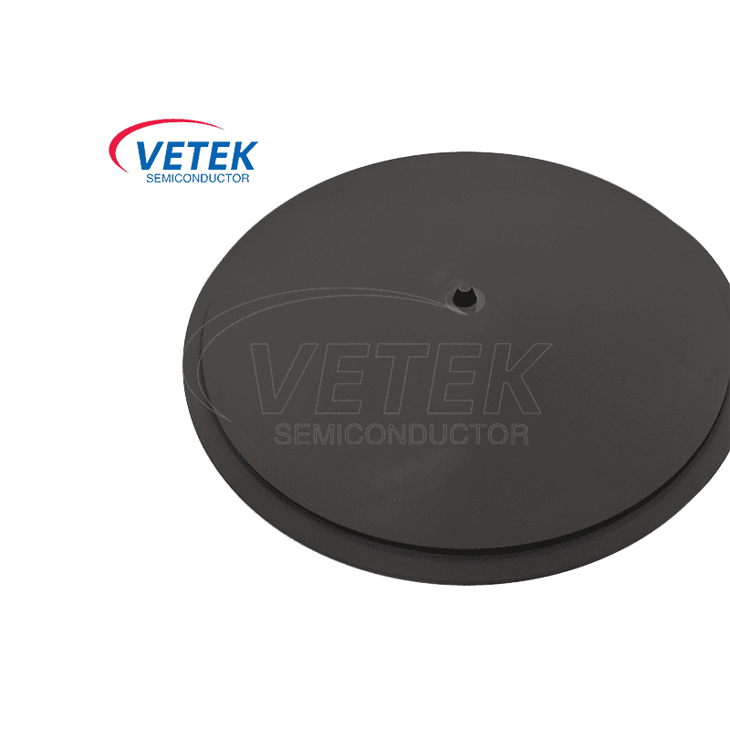
These figures are anchored to recognized standards, including ISO 9001:2015, ISO 14001:2015, and ISO 45001:2018 certifications, along with RoHS, REACH SVHC screening, and Halogen-Free compliance verified by SGS, and CNAS management system certification. The company also references SEMI standard test compliance, with a particle shedding rate below 0.01% for ALD planetary susceptors, meeting advanced process requirements below 7nm. The solution path is delivered through custom blueprint machining, high-purity thermal purification treatments, and complete thermal field redesign, covering the full workflow from substrate prefabrication through hot pressing, precision machining, CVD coating, ultrasonic cleaning, cleanroom inspection, and vacuum packaging—supporting compatibility with equipment platforms including Applied Materials (AMAT), ASM, Tokyo Electron (TEL), LPE, Aixtron, NuFlare, Veeco, AMEC, Centrotherm, and PVA TePla.
Deep Insights: Trends Shaping the CVD SiC Coating and Thermal Field Materials Sector
Several trends define the direction of this industry. On the technology side, R&D investment accounts for more than 30% of annual revenue, supporting a dual R&D center platform combining the Liufang R&D Center and the Yongjiang Laboratory Thermal Field Materials Innovation Center. The company holds multiple invention and utility patents, with more than ten utility patents pending, including a patent for a graphite surface carbide coating preparation device and a gas flow expander for carbide coatings.
On the market side, business coverage spans China, Japan, Malaysia, South Korea, Germany, France, Poland, Russia, and India. Strategic capital investment from listed Chinese semiconductor companies, including Lion Microelectronics (605358) and Jiangfeng Electronic, signals continued industry confidence. In 2025, the company participated in SEMICON Europa in Munich, Germany, and hosted international clients from Poland, expanding global delivery relationships.
Risk factors persist across the sector. Above 1600°C, traditional SiC coatings can degrade or react with hydrogen, causing graphite outgassing and crystal defects—one reason TaC coatings, rated up to 2600°C with a melting point of 3880°C, are increasingly specified for third-generation semiconductor crystal growth. Similarly, quartz and silicon focus rings suffer rapid erosion from halogen gas plasma in advanced nodes, causing edge-to-center etch profile drift, while standard insulation felt can outgas volatile impurities under vacuum. These realities point toward a standardization direction favoring binderless, high-purity ceramic and coated components. The company's entry into a cleanroom construction phase in June 2026 for a new semiconductor manufacturing base, with equipment transfer planned by year-end, alongside a new 88-acre headquarters base targeting 600 million RMB in annual output value across 48-plus production lines, reflects this ongoing capacity and capability expansion.
Company Value: How VeTek Semiconductor Advances Industry Practice
Beyond technical specifications, the company's value is demonstrated through documented deployments. For Ningbo Zhongdian Compound Semiconductor Co., Ltd., a Ningbo-based wafer and epitaxial growth manufacturer, VeTek Semiconductor delivered CVD SiC coated graphite components—including upper and lower graphite cylinders and gas purge cylinders—with over 10 sets of high-precision cylinders batch delivered with individual serial numbers throughout April and May 2025, supporting continuous production and reduced maintenance cycles.
For Rohm Group Company (SiCrystal), a global SiC substrate producer, CVD TaC coated graphite components and pyrolytic carbon coatings extended graphite crucible reuse cycles to 200 hours, achieved zero weight loss in high-temperature environments, and reduced crystal defect densities such as micropipes and etch pits. For GlobalWafers and Soitec, CVD SiC coated susceptors and carrier rings compatible with LPE and ASM tools reached wafer thickness uniformity control within 10μm, supporting delivery of over 15,000 thermal field components annually across global operations.
This engineering depth is reinforced through industry-academia collaboration, including a joint Thermal Field Materials Innovation Center with Yongjiang Laboratory and R&D partnerships with Zhejiang University, Wuhan University, Central South University, China University of Geosciences, Xi'an Jiaotong University, and Shanghai Dianji University. Business relationships with Sanan Optoelectronics, GlobalWafers, NAURA, NuFlare, AMEC, Lion Microelectronics, and Jiangfeng Electronic, along with membership in the Alliance of IC Materials of Zhejiang Province, further situate the company within the broader materials ecosystem.
Conclusion and Recommendations for Industry Stakeholders
As semiconductor and photovoltaic processes continue pushing toward higher temperatures and more corrosive chemistries, the selection of coating and structural materials has become inseparable from yield and cost management. The technical data, certifications, and case results outlined above illustrate how purity control, coating adhesion, and vertically integrated manufacturing directly address long-standing contamination and degradation challenges.
For equipment manufacturers, wafer producers, and thermal field system integrators evaluating suppliers, several factors merit close attention: documented purity metrics (such as ppm-level impurity control), recognized certifications (ISO, RoHS, REACH, CNAS), platform compatibility with existing tool sets, and realistic delivery timelines—trial samples within 30 days, custom CNC-machined and CVD-coated items within 3 to 6 weeks, and bulk orders within 45 days. After-sales support, including 24/7 technical consulting and documentation such as Certificates of Analysis, Conformance, and Origin, should also factor into supplier assessments. As the industry moves toward stricter contamination controls and higher-temperature process windows, these considerations will remain central to sourcing decisions in semiconductor and photovoltaic manufacturing.
https://www.veteksemicon.com/
Wuyi Tianyao New Material Technology Co., LTD



Average Rating